The Tunnel FET
In accordance with Moore’s Law, metal oxide semiconductor (MOS) field effect transistors (FETs) have experienced steady, exponential downsizing of their critical dimensions. As the size was reduced, operating voltage was also reduced to maintain constant electric fields. However, the voltage did not scale at the same rate as transistor size. For conventional MOSFETS, there is a fundamental limit on the operating voltage set by the minimum inverse subthreshold slope (S) of 60 mV/dec at room temperature. A value of S = 60 mV/dec means that 60 mV of gate voltage is required to reduce the current by an order magnitude. If an ON/OFF current ratio of 104; is desired, and if we assume that two-thirds of the maximum gate voltage is required to obtain a high ON current, the supply voltage cannot be reduced below 720 mV. Reducing the voltage range below this would either mean degraded ON current or increased leakage current. Thus, the voltage scaling cannot keep pace with the aggressive transistor scaling. As a result, IC power consumption is rising fast, and it has become a limiting factor to continued scaling.
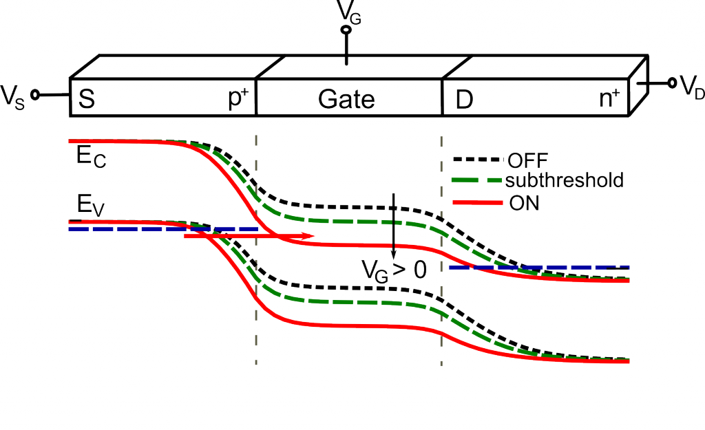
Top: schematic diagram for a p-i-n TFET. Bottom: energy band diagrams in three modes of operation.
Tunnel Field Effect Transistors (TFETs) have been proposed as an effective way to circumvent the fundamental limit of S. Here is how a TFET works: in the off state, the channel conduction band, Ec,g is above the source valance band, Ev,s creating a large tunneling barrier for valance band electrons in the source. In subthreshold, when the bands are crossing, a channel opens for the electrons, and S can be below the thermal limit. In the on state, Ev,s − Ec,g > 0 and the valance band states are aligned with the empty conduction band states enabling significant Zener tunneling of electrons through the barrier. Unlike conventional MOSFETs where the current limiting barrier is a ‘thermal’ barrier, here, current is limited by a ‘tunnel’ barrier. This makes it possible to achieve inverse subthreshold swings below 60 mV/dec and holds promises for keeping Moore’s Law alive.
Tunnel FETs have shown interesting characteristics for use as future alternate logic devices and they have been listed as one of the emerging research devices by the International Technology Roadmap for Semiconductors (ITRS). However, there are practical design issues that need consideration before making chips out of TFETs. Therefore, in accordance with the growing interest for using the TFET as the next generation switch, my PhD dissertation is focused on the quantum mechanical simulation of TFETs at the nanometer scale to address some of the critical design issues for their practical implementation.